Q-For common emitter configuration, which of the following is the correct relation?
a) IC < IE
b) IC = βIB
c) IC = αIE
d) IC = IE
…………..
Answer: d
Explanation: All the relations hold true i.e. IC = βIB and IC = αIE. As α<1, hence IC < IE.
Q-For a BJT, for common base configuration the input characteristics are represented by a plot between which of the following parameters?
a) VBE and IE
b) VBE and IB
c) VCE and IC
d) VCC and IC
…………..
Answer: a
Explanation: The input signal is applied between the base and the emitter terminals. Input current flowing is the base current and hence characteristics are represented by a plot between VBE and IB.
Q-For a BJT, for common base configuration the output characteristics are represented by a plot between which of the following parameters?
a) VBE and IB
b) VCE and IC
c) VCB and IC
d) VCE and IB
…………..
Answer: c
Explanation: The input signal is applied between the collector and the emitter terminals. Input current flowing is the collector current and hence characteristics are represented by a plot between VCE and IC.
Q-Considering the resistances of emitter, collector and base to be Re, Rc and Rb respectively, which of the following is the correct statements?
a) Re > Rb > Rc
b) Rc > Rb > Re
c) Rb > Rc > Re
d) Rb = Rc > Re
………..
Answer: c
Explanation: As the base is lightly doped, the number of free charge carriers are less and hence the resistance is high and as the emitter is the most highly doped, its resistance is low
Q-Which of the following currents in a BJT is also called leakage current?
a) IC
b) IE
c) ICO
d) ICBO
………….
Answer: a
Explanation: Leakage current in BJT is represented by ICO, which is due to the flow of minority carriers in the transistor. It consists of ICBO and ICEO. ICO depends on temperature, doubling with 10° rise in temperature. It thus effects total collector current, IC, and hence affects the power dissipation.
Q-For a BJT, what is typically the shape of the power dissipation curve, if it’s plotted on the output characteristics?
a) Parabola
b) Linear
c) Hyperbola
d) Circular
………….
Answer: c
Explanation: Power Dissipation in a BJT is given by P=VCE.IC. This is in the form of k=xy which is the equation of a hyperbola.
Q-What is the region on the output characteristics below IC = ICEO line called?
a) Active region
b) Cutoff region
c) Saturation region
d) Active & Saturation region
………..
Answer: b
Explanation: The region below IC = ICEO is called the cutoff region.
Q-What is the region on the output characteristics for VCE < VCEsat called?
a) Active region
b) Cutoff region
c) Saturation region
d) Active & Cutoff region
…………
Answer: c
Explanation: The region below VCE < VCEsat is called the saturation region.
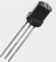
Q-For the given transistor, what is the correct sequence of the pins from left to right?

a) ECB
b) BCE
c) CEB
d) CBE
……………
Answer: d
Explanation: With the curved side facing us, the answer can either be collector-base-emistter, left to right, or emitter-base-collector. Hence the correct option is CBE, and that applies for an NPN transistor.
next page//